NVIDIA Introduces NVHBM for Custom AI Accelerators
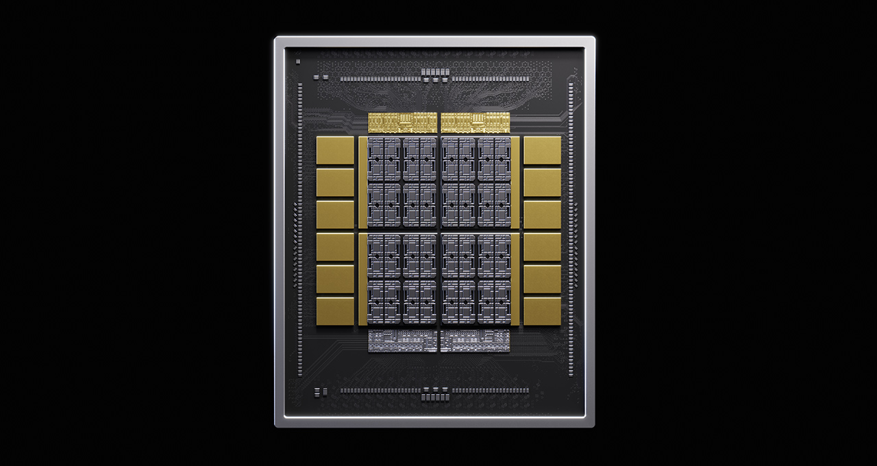
NVIDIA introduced NVHBM on August 26, moving a custom memory controller from an XPU die into the HBM base die. NVIDIA claims the design delivers up to 30% more bandwidth, 15% lower HBM power use, and up to 25% more XPU compute-die area than standard HBM4E. Amazon's Annapurna Labs is the first NVHBM collaborator, with Trainium4 linked to the broader NVLink Fusion program.
NVIDIA introduced NVHBM, a custom high-bandwidth memory architecture that places NVIDIA's memory controller in the base die of a 3D HBM stack rather than on an XPU's main compute die. The company announced the technology on August 26 as an extension of its NVLink Fusion program for integrating custom processors into NVIDIA rack-scale infrastructure.
According to NVIDIA, NVHBM delivers up to 30% more memory bandwidth per stack, 15% lower HBM power consumption, and up to 25% more area on the XPU compute die than standard HBM4E. Those figures are NVIDIA performance claims, not independently benchmarked results.
The architectural change moves controller and interface logic from the accelerator die into the HBM stack's base die. NVIDIA states that conventional HBM designs place the controller on the XPU, consuming silicon area that could otherwise be used for compute. Its technical material further claims NVHBM can reduce PHY and support area by up to 67% relative to JEDEC HBM4E, while narrower interfaces can simplify interposer routing.
Trainium4 is the first named collaboration
Amazon's Annapurna Labs is the first company named as an NVHBM collaborator. NVIDIA's announcement states that Annapurna Labs will work on NVHBM and NVLink scale-up architecture as part of the companies' broader NVLink Fusion collaboration. NVIDIA also reports that Annapurna Labs will support NVLink Fusion with its next-generation Trainium chips, starting with Trainium4.
"NVHBM represents a new architectural approach to advancing high-bandwidth memory performance and efficiency," Nafea Bshara, vice president of Annapurna Labs at Amazon, said in NVIDIA's announcement. "We look forward to this technology collaboration to benefit future AWS infrastructure designs."
NVIDIA said it is establishing a standard NVHBM implementation that will be available from multiple memory providers. The company frames that approach as a way to reduce memory integration and qualification work for NVLink Fusion customers developing custom AI chips.
A targeted alternative to commodity HBM
NVLink Fusion is NVIDIA's framework for connecting partner XPUs and CPUs with NVIDIA's scale-up fabric and MGX rack-scale systems. Tom's Hardware characterizes NVHBM as a building block for custom-silicon partners rather than a replacement for commodity HBM. NVIDIA's own materials state that the technology is based on the same approach it intends to use in future GPUs.
The memory-bandwidth claim is particularly relevant to memory-bound inference and training workloads, where model weights, activations, and KV cache reads can constrain accelerator utilization. Higher bandwidth can raise throughput only when memory transfer is the limiting factor; realized application gains also depend on model architecture, precision, batch size, software kernels, interconnect behavior, and system-level power limits.
For accelerator designers, moving interface logic off the main die illustrates a broader packaging trend: advanced-memory integration is becoming a design variable alongside compute cores and networking. Companies pursuing comparable rack-scale systems often weigh the benefits of custom memory interfaces against supplier qualification, packaging complexity, and software compatibility. NVIDIA's multi-provider implementation proposal addresses one part of that tradeoff, but public reporting has not disclosed NVHBM pricing, memory-vendor availability, Trainium4 specifications, or production timing.
Key Points
- 1NVIDIA moves the HBM controller into the stack base die, claiming higher bandwidth and more XPU silicon area than HBM4E.
- 2Amazon's Annapurna Labs is NVHBM's first named collaborator, linking Trainium4 to NVIDIA's NVLink Fusion rack-scale ecosystem.
- 3For memory-bound AI workloads, bandwidth improvements matter most when model weights or KV cache access constrains accelerator throughput.
Scoring Rationale
NVHBM is a notable AI infrastructure development because memory bandwidth, package area, and power are central constraints for large-scale training and inference accelerators. Its practical impact depends on adoption by memory suppliers and custom-silicon partners, plus independently demonstrated system-level performance.
Sources
Primary source and supporting public references used for this report.
View 5 more sources
- NVIDIA NVLink Fusion Brings NVHBM to Next-Generation AI Infrastructure | NVIDIA Technical Blogdeveloper.nvidia.com
- Nvidia custom 'NVHBM' promises 30% higher bandwidth, 15% lower power than commodity HBM4e — custom base die and PHY will be available to NVLink Fusion partnerstomshardware.com
- Nvidia expands NVLink Fusion strategy to supercharge custom silicon memorysdxcentral.com
- NVIDIA Develops Custom “NVHBM” Memory For AI, Claiming 30% More Bandwidth and 15% Lower Power Than HBM4Ewccftech.com
- NVIDIA NVHBM Moves the Memory Controller Into the HBM Stack, With Amazon’s Trainium4 First in Linestoragereview.com
Practice interview problems based on real data
1,625 SQL & Python problems across 15 industry datasets — the exact type of data you work with.
Try 250 free problems