Netrasemi launches A2000 12nm edge AI chip
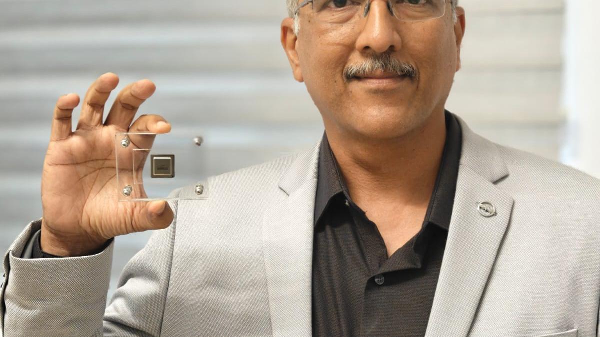
Kerala-based fabless startup Netrasemi, backed by Zoho, launched its flagship edge AI system-on-chip, the A2000, after successful silicon bring-up, according to reporting by TimesTech and The Economic Times. The A2000 was fabricated at TSMC on a 12nm process node and integrates in-house neural processing, vision processing, image signal processing and crypto engines, per company statements reported by those outlets. The startup is running early trials with three customers in surveillance and automotive, and multiple outlets report volume commercial production is targeted for 2027 at TSMC. Netrasemi has raised Rs 125 crore to date and was among the first four startups to receive Rs 15 crore under India's MeitY Design Linked Incentive (DLI) scheme. Industry observers see it as a practical step toward India-built edge AI silicon rather than a frontier-node chip.
What happened
Netrasemi, a Kerala-based fabless semiconductor startup backed by Zoho, announced the launch of its flagship edge AI system-on-chip, the A2000, after achieving successful silicon bring-up, according to reporting by TimesTech and The Economic Times. The A2000 was fabricated at TSMC on a 12nm process node and is described in those reports as integrating in-house neural processor units, vision processing units, image signal processors and crypto engines. The company is running early customer trials, including with three customers in surveillance and automotive, and multiple outlets report that volume commercial production is targeted for 2027 at TSMC. TimesTech and The Economic Times also report that Netrasemi has raised Rs 125 crore to date and was among the startups that received Rs 15 crore under India's MeitY Design Linked Incentive programme.
Technical context
Per company statements reported by TimesTech and The Economic Times, the A2000 targets on-device AI for smart cameras, edge AI boxes and intelligent video gateways and includes what the reporting calls a proprietary heterogeneous graph-stream parallel processing architecture, alongside hardware acceleration IP for neural processing, vision, image handling and secure boot. Companies building edge AI silicon commonly favor domain-specific accelerators and power efficiency over bleeding-edge process nodes; using a 12nm node from TSMC allows faster time-to-market for a specialized SoC while keeping wafer costs lower than leading-edge nodes, and pairing multiple dedicated engines mirrors global edge-silicon designs optimized for vision and streaming workloads.
Industry context
India's semiconductor policy incentives, including MeitY's DLI and Design Infrastructure Support, are intended to seed domestic chip design capability, and reporting by TimesTech and The Economic Times links those programmes directly to Netrasemi's development milestones. While the A2000 is not a frontier-node AI accelerator, it represents a supporting step in building a local design ecosystem and supplier relationships with foundries such as TSMC.
For practitioners
For system integrators working on surveillance, robotics and industrial automation, a locally designed SoC with claimed power and I/O features could simplify productization and compliance, though adoption depends on long-term supply and software support. Teams evaluating the part should treat performance and power claims as vendor-reported until independent benchmarks or OEM deployment data are available.
What to watch
- •Productization and benchmarks: independent measurements or OEM benchmark data confirming the A2000's performance and power envelope.
- •Production milestones: reports from TSMC, the company, or OEM partners verifying volume shipment timing and yields.
- •Software and tooling: availability of SDKs, runtimes and model-quantization tooling to deploy common vision models on the A2000.
- •Follow-on chips: reporting indicates Netrasemi is developing an IoT-targeted R1000 MCU (with the College of Engineering Trivandrum under MeitY's Chip-to-Startup programme) and an edge AI server chip, A4000; track fabrication timelines and partner disclosures for those parts.
Key Points
- 1Netrasemi shipped silicon for its A2000 edge AI chip on a 12nm TSMC process, prioritizing time-to-market over leading-edge node performance.
- 2Government incentives, including Rs 15 crore under MeitY's Design Linked Incentive scheme, helped fund development of the domestically designed chip.
- 3Commercial adoption will depend on production yields, OEM integrations, and software tooling rather than raw process-node leadership.
Scoring Rationale
A domestically designed edge AI SoC reaching silicon and early customer trials is notable for practitioners focused on embedded AI and supply-chain diversification. The chip uses an established 12nm node and depends on TSMC fabrication and OEM integrations, limiting immediate disruption but marking a meaningful, well-corroborated step for India's chip design ecosystem (score held from prior audit; core figures corroborated via search).
Sources
Public references used for this report.
Practice interview problems based on real data
1,625 SQL & Python problems across 15 industry datasets — the exact type of data you work with.
Try 250 free problems