Google Reportedly Develops Frozen v2 Chip for Gemini Inference
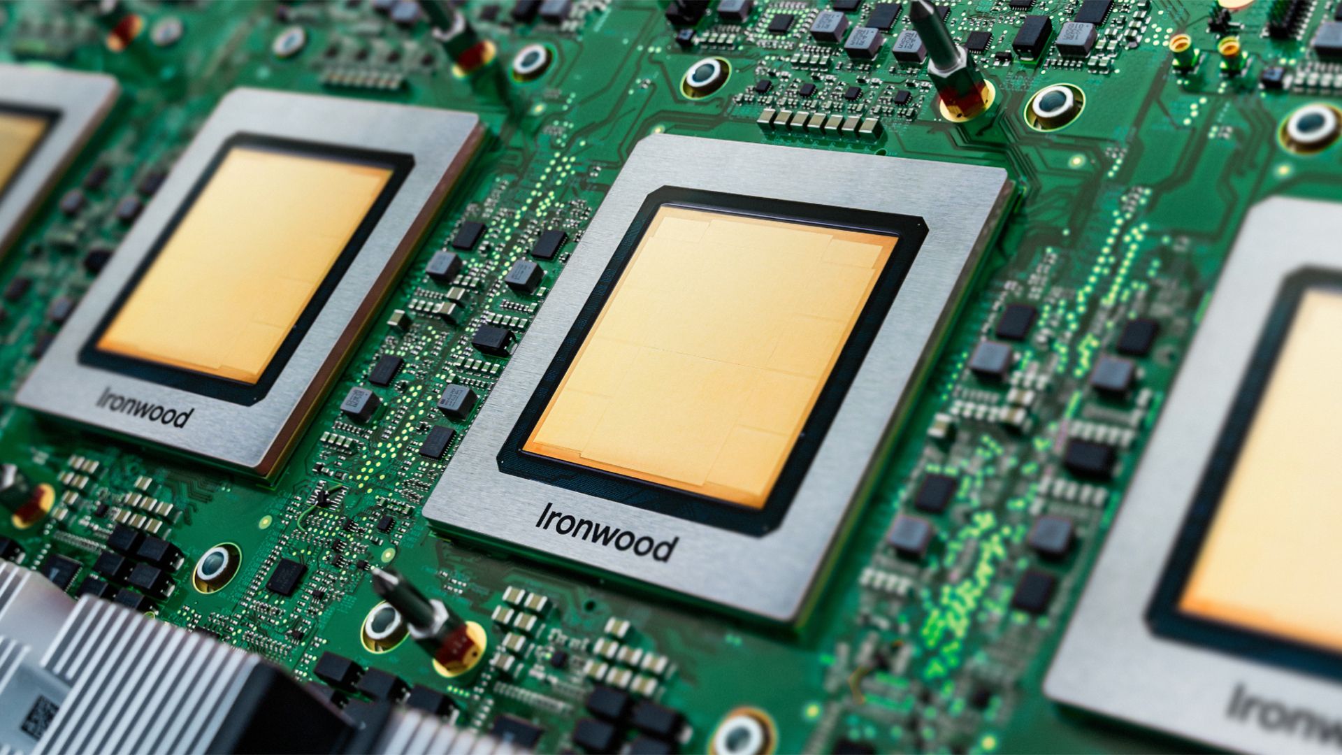
Google is reportedly developing Frozen v2, an experimental server chip that would embed parts of Gemini's architecture in silicon. Internal projections cited by The Information put its efficiency at six to ten times more tokens per unit of power than Google's newest TPUs, but the project is not an announced product and may not reach deployment.
Google is reportedly developing a server chip called Frozen v2 to run Gemini models with less computation and data movement. The project could reach deployment in 2028, but it is still experimental and its performance claims have not been independently benchmarked.
A model-specific chip, not another general TPU
The Information reported on July 20, citing two people with direct knowledge of the work, that Frozen v2 would permanently embed parts of Gemini's architecture into the chip. Google engineers project that the design could serve six to ten times more tokens per unit of power than the company's newest tensor processing units, according to the report. That figure is an internal projection, not a published benchmark.
The reported design is narrower than a general-purpose TPU. It is intended to reduce calculations and data movement for a known model architecture, while Google's existing TPUs support a broader range of training and inference workloads. The Information said Google currently views Frozen v2 partly as a trial and does not plan to produce it at the same scale as its TPU line.
Reuters separately reported the story and obtained a statement from Alphabet saying its teams continually research efficiency improvements, while cautioning that experimental projects face technical and business reviews and do not all reach production. Reuters also reported that Alphabet shares rose about 3% after the report. The market move does not validate the engineering claims.
Efficiency comes with an architecture constraint
A model-specific accelerator could lower inference power and cost by eliminating flexibility that a general chip must preserve. The trade-off is longevity: future Gemini versions would need to retain the same underlying architecture for the chip to remain useful, although model weights could still change.
For ML infrastructure teams, the relevant question is not the code name or the stock reaction. It is whether Google can demonstrate better tokens per watt on representative workloads without locking model development to a silicon design years before deployment.
What to watch
There is no public specification, benchmark suite, manufacturing plan, or product commitment for Frozen v2. Watch for an official Google disclosure, reproducible latency and energy measurements, compiler and serving-stack details, and evidence that the design survives changes to Gemini's architecture. Until then, the reported 2028 target and efficiency range should be treated as plans and projections rather than shipped capability.
Key Points
- 1The Information reports that Google is developing Frozen v2, a server chip that would embed parts of Gemini's architecture directly in silicon.
- 2Google engineers project six to ten times more tokens per unit of power than the newest TPUs, but no independent benchmark or public specification supports that estimate yet.
- 3The reported 2028 project trades hardware flexibility for inference efficiency and may remain a trial rather than a production product.
Scoring Rationale
A potentially material change to Google's inference architecture could affect serving cost, energy demand, and custom-silicon competition, but the project is experimental, targets 2028, and currently rests on one originating report plus a separately retrieved Alphabet response.
Sources
Public references used for this report.
Practice interview problems based on real data
1,625 SQL & Python problems across 15 industry datasets — the exact type of data you work with.
Try 250 free problems