Google Engages Samsung for Icefish TPU Component

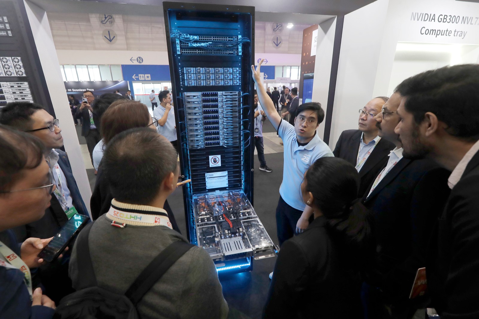
Reporting by Reuters and The Information says Alphabet's Google is in talks with Samsung Electronics to manufacture part of its next-generation tensor processing unit, codenamed "Icefish." Reuters reports TSMC would produce the main compute die while Samsung would make a memory-facing I/O die using its 2-nanometer process, and that Google is working with MediaTek on the design. Multiple outlets cite 2028 as a potential target for mass production. Reuters also reports Google has explored Intel for large-volume TPU manufacture and that Samsung declined to comment while Alphabet did not respond. The coverage frames the discussions as part of broader efforts to ease reliance on TSMC amid industry capacity pressure.
What happened
The Information reports that Alphabet's Google is in talks with Samsung Electronics to have Samsung manufacture part of its next-generation tensor processing unit, codenamed "Icefish." Reuters reports that Google plans for TSMC to fabricate the main compute die while Samsung would produce a memory-facing I/O die using its 2-nanometer process. Reuters and TrendForce report that the Icefish program is being developed with chip designer MediaTek and that mass production is being eyed as early as 2028. Reuters also reports Google has separately discussed large-volume TPU manufacturing with Intel. Reuters notes Samsung declined to comment and that Alphabet did not immediately respond to requests for comment.
Technical context
High-performance AI accelerators typically divide functionality across a high-density compute die and companion dies or packages that handle memory interfaces, power management, and I/O. Using a leading-edge node for an I/O or HBM-adjacent die is unusual but not unprecedented when a vendor can integrate advanced packaging and memory expertise. Reports that Samsung could supply HBM, the I/O die, and advanced packaging are consistent with vertically integrated offers other vendors have pitched to hyperscalers.
Industry context
Public reporting frames these negotiations as part of a broader push by cloud and chip customers to reduce single-supplier concentration, because TSMC is approaching full utilization from surging AI demand. Suppliers with both memory and foundry capabilities, and with packaging ecosystems, can present turnkey value to large AI chip buyers. TrendForce and other trade outlets highlight Samsung's recent wins, including a reported $16.5 billion order from Tesla, as background for its foundry momentum.
What to watch
Observers will track three indicators:
- •whether Google publicly confirms a split supply chain and the specific dies allocated to each foundry
- •qualification timelines and packaging demonstrations that show Samsung can meet Google's HBM and interposer specs at scale
- •capacity ramp schedules for Samsung's Texas fab and TSMC's 1.4-nanometer programs as cited in trade reporting
Additional confirmations from Google partners such as MediaTek or from contract announcements would materially raise confidence in the reported arrangement.
For practitioners
If multi-supplier manufacturing for large AI accelerators becomes more common, engineering teams should expect greater heterogeneity in packaging, thermal behavior, and supply-chain traceability. Systems teams and performance engineers will likely need earlier co-validation of packaging and memory subsystems when dies originate from different fabs.
Key Points
- 1Reported talks split Icefish production: TSMC for the main compute die, Samsung for a 2nm memory I/O die, easing single-supplier pressure.
- 2Samsung's combined memory, foundry, and packaging capabilities make it a logical candidate for HBM-adjacent die work, potentially shortening integration paths.
- 3Industry observers note multi-fab TPU supply chains increase integration and validation burdens for system builders and performance engineers.
Scoring Rationale
The reported talks directly affect AI hardware supply chains and foundry competition, with Reuters and The Information as primary sources and corroboration from TrendForce and The Elec. The story is notable for AI infrastructure practitioners but awaits confirmation from either party before reaching higher significance.
Sources
Public references used for this report.
View 14 more sources
- [News] Samsung Reportedly in Talks for Google 2nm TPU I/O Die Order; 2028 Mass Production Eyedtrendforce.com
- Samsung likely to make part of Google's Icefish AI chip after winning ...kedglobal.com
- Google to entrust next-gen AI chip production partly to Samsungchosun.com
- Google koennte zur Fertigung neuer TPU-Generation neben TSMC auch Samsung nutzenheise.de
- Google linked with Samsung deal for next-gen AI chipmobileworldlive.com
- Samsung could make a part of Google's next-gen AI chip using 2nm techsammobile.com
- Samsung manufacturing Google TPU components using 2nm technologytechnews.tw
- Taiwan Semiconductor faces capacity shortages; Google's TPU reportedly introduced Samsung as a contract manufacturer for the first timenews.futunn.com
- Google Eyes Samsung's 2nm Process for 'Icefish' TPU - Sammy Hubsammyhub.com
- Samsung Poised to Land Google's Next-Gen AI Chip 'Icefish'finance.biggo.com
- Google Partners with Samsung and TSMC for Advanced Icefish AI Chipintellectia.ai
- GOOGL Explores Samsung Partnership For Next-Gen AI Chip Amid TSMC Capacity Crunchstocktwits.com
- Google Seeks Samsung Capacity for Next-Gen TPUletsdatascience.com
- Will Samsung Make New Google 'Icefish' TPU?forbes.com
Practice with real Ad Tech data
90 SQL & Python problems · 15 industry datasets
250 free problems · No credit card
See all Ad Tech problems