Sandisk and SK hynix Publish First HBF Specification
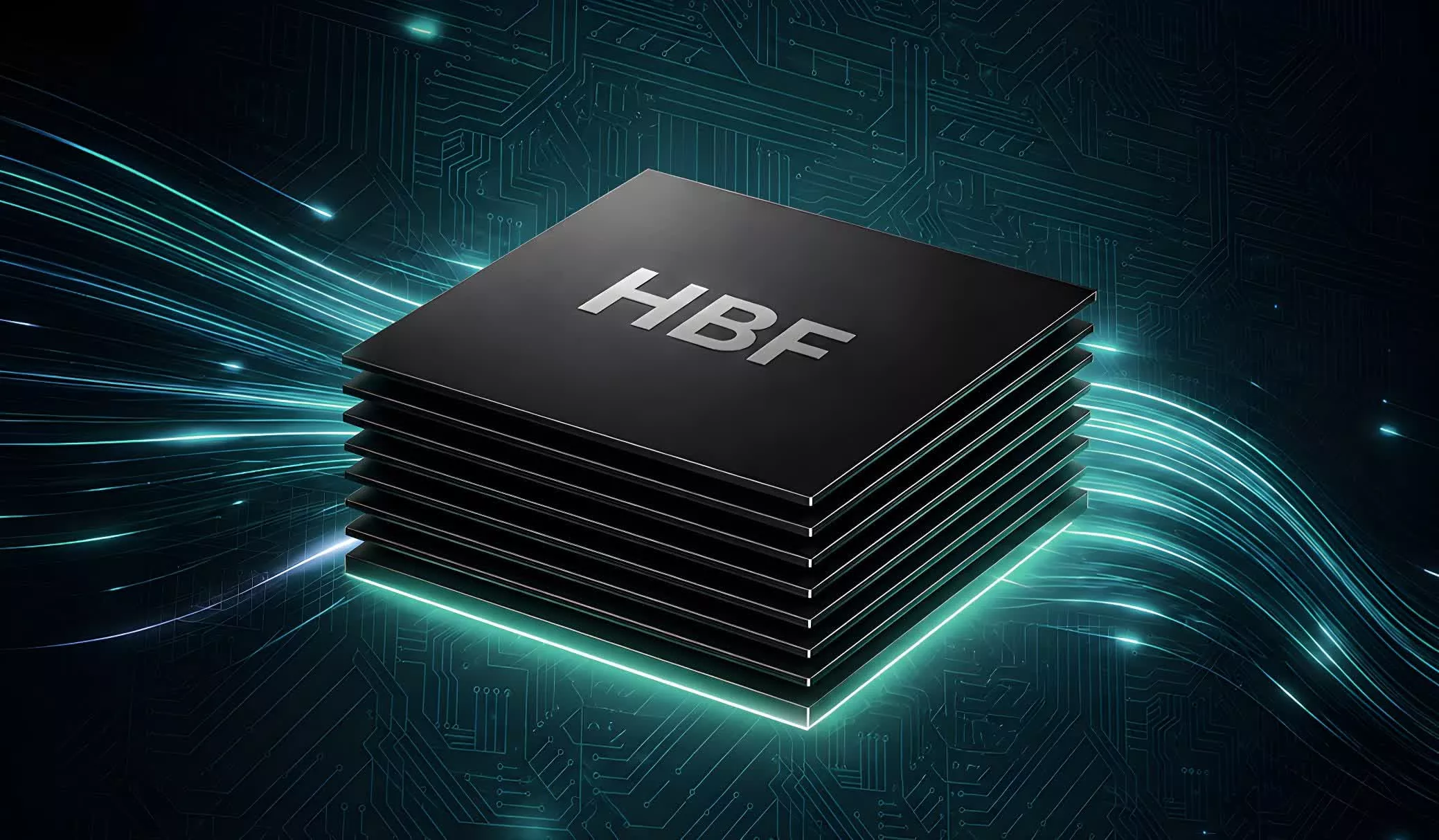
Sandisk and SK hynix released the first Open Compute Project technical specification for High Bandwidth Flash on August 3-4. The open framework covers the xPU-HBF host interface, electrical design, packaging, reliability and software operations. SK hynix says the outlined configurations reach 512 GB and span about 0.4 to 3.0 TB/s, but the release is a standard rather than a commercial product launch.
Sandisk and SK hynix released the first High Bandwidth Flash (HBF) technical specification through the Open Compute Project on August 3-4. The companies say the open framework is intended to help accelerator and system designers integrate a NAND-based, high-capacity memory tier close to compute for AI inference.
Sandisk says the specification defines the system interface, electrical and baseline performance guidance, the xPU-HBF host interface, reliability and packaging requirements for an HBF die stack, and a software guide for read and write operations. Sandisk and SK hynix were the primary contributors. Google and Tenstorrent joined the workstream during the standardization process and contributed to validation, according to both companies.
What the specification defines
SK hynix says the standard describes 8-high and 16-high NAND stack configurations with capacity up to 512 GB. It places bandwidth into three grades spanning approximately 0.4 TB/s to 3.0 TB/s and uses the Universal Chiplet Interconnect Express, or UCIe, to connect HBF with processors such as CPUs and GPUs. These figures describe configurations in the specification, not measured performance from a broadly available commercial product.
HBF is designed to add a larger NAND-based tier alongside high-bandwidth memory rather than replace HBM in every role. HBM remains the lower-latency tier close to an accelerator, while HBF is intended to hold larger model data nearer to compute than conventional storage. Independent reports from SDxCentral and TechSpot describe the release as a step toward wider system experimentation, but neither establishes production availability or workload-level gains.
The remaining engineering questions
An open interface can reduce integration friction across memory, accelerator and server vendors. It does not by itself solve the software problems in a tiered-memory system. Real results will depend on data placement, caching, access patterns, endurance, latency and application support.
The immediate event is therefore a standards milestone. It gives system designers a common technical baseline to evaluate while leaving commercial schedules, conformance testing and independent performance results for later releases.
Key Points
- 1Sandisk and SK hynix published the first OCP HBF specification for NAND-based near-compute memory in AI inference systems.
- 2SK hynix says the outlined configurations reach 512 GB and approximately 0.4 to 3.0 TB/s; those are specification figures, not independent product benchmarks.
- 3The open interface advances interoperability, while commercial availability and workload-level performance remain unverified.
Scoring Rationale
This is a notable AI-infrastructure standard because inference deployments increasingly face memory-capacity and bandwidth constraints. It does not yet represent a commercial product launch, but the OCP interface can affect future accelerator, server, and memory-hierarchy designs.
Sources
Primary source and supporting public references used for this report.
View 3 more sources
Practice interview problems based on real data
1,625 SQL & Python problems across 15 industry datasets — the exact type of data you work with.
Try 250 free problems