Tesla Demonstrates AI5 Processor, Claims 40X Boost
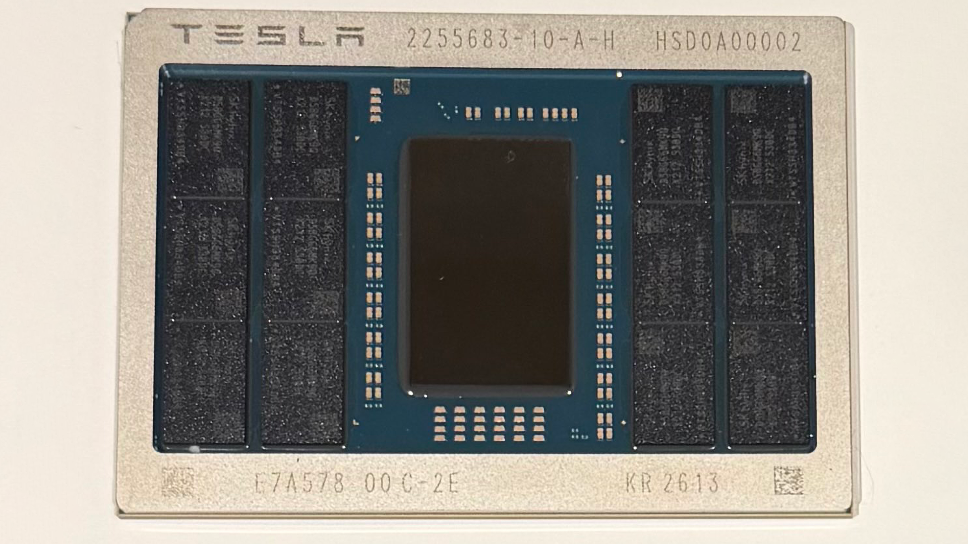
Elon Musk unveiled a first sample of Tesla's AI5 processor, claiming up to a 40X performance improvement over AI4 in certain workloads. The module reportedly uses a compact ASIC die, an organic substrate, and twelve SK hynix memory packages, likely GDDR6 or GDDR7, implying a wide memory interface (about 384-bit if each package is a single 32-bit device). Musk thanked Samsung and mistakenly thanked a Twitter handle @TaiwanSemi_TSC rather than TSMC. Tesla positions AI5 for vehicles, Optimus robots, and potential xAI datacenter use, and said AI6 and Dojo 3 are in development. Key unknowns remain: the actual memory configuration, sustained throughput versus peak claims, power efficiency, and which foundry will handle volume production.
What happened
Elon Musk showcased an early sample image of Tesla's new AI5 processor and claimed it can be up to 40X faster than AI4 in some scenarios. The sample is a compact ASIC on an organic substrate surrounded by 12 memory packages from SK hynix, and Musk publicly thanked Samsung and a Twitter handle, mistakenly writing @TaiwanSemi_TSC rather than TSMC. He also named AI6 and Dojo 3 as future projects.
Technical details
The observable hardware and Musk's comments give practitioners a few concrete signals and several open questions. The visible module uses a relatively small ASIC die, which Musk described as about half a reticle-size compared with prior designs. The memory packaging implies a wide I/O:
- •If the 12 packages are GDDR6/7 and each is a 32-bit device, the interface would be approximately 384-bit.
- •The module uses an organic substrate and industry-standard memory, not proprietary HBM stacks, which favors cost and manufacturability at scale.
- •Packaging choice hints at a tradeoff: smaller die area per chip, higher memory-pin count via discrete packages, and a focus on throughput per module rather than single-die monolithic memory bandwidth.
Context and significance
Tesla is pursuing vertical integration across hardware and software for vehicles and robotics, and a bespoke AI ASIC aligns with that strategy. A smaller die with industry-standard memory can lower per-unit cost and enable high-volume production if the foundry path and yield are favorable. A claimed 40X jump over AI4 is meaningful if it reflects real-world throughput or efficiency, but the claim needs independent benchmarks. Compared with industry peers, Tesla appears to prioritize packaging and system-level bandwidth over adopting HBM-heavy tiles; that changes cost, thermal, and board-level tradeoffs. Musk's mistaken thank-you to @TaiwanSemi_TSC highlights ongoing ambiguity around production partners; public signals mention Samsung and SK hynix involvement.
What to watch
Validate the performance and power numbers with third-party benchmarks, confirm the foundry partner and production node, and watch whether Tesla scales packaging yields for automotive and robot deployments. The true impact depends on sustained throughput, thermals, and cost per TOPS when integrated into vehicles and Optimus robots.
Key Points
- 1Tesla showcased an AI5 sample claiming up to 40X performance vs AI4, signaling aggressive hardware iteration for vehicles and robots.
- 2Module uses a small ASIC plus 12 SK hynix memory packages, suggesting a wide 384-bit-class memory interface with GDDR6/7 tradeoffs.
- 3Foundry and validation remain open: Samsung and SK hynix are visible partners, while TSMC's role is unclear and independent benchmarks are needed.
Scoring Rationale
Hardware sample and bold performance claim are notable for practitioners focused on AI infrastructure and edge robotics, but the announcement lacks independent validation and production clarity. That reduces immediate technical impact.
Sources
Public references used for this report.
Practice interview problems based on real data
1,625 SQL & Python problems across 15 industry datasets — the exact type of data you work with.
Try 250 free problems