SK Hynix Considers Miyagi Memory Chip Plant
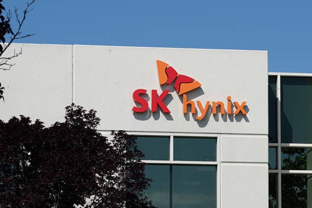
SK Hynix was reported by Reuters on August 21 to be considering a memory-chip manufacturing plant in Miyagi prefecture, Japan, with a possible investment of tens of trillions of won. The company told Reuters that no decision had been made and that locations with the required infrastructure could be candidates, while the reported project would be the first large-scale Japanese manufacturing investment by a South Korean chipmaker if completed.
SK Hynix is considering building a memory-chip manufacturing plant in Japan's Miyagi prefecture, Reuters reported on August 21, citing South Korean newspaper Hankyoreh. The potential project could involve investment of tens of trillions of won, according to the Reuters account.
SK Hynix told Reuters that no decision had been made. "Any location with the necessary infrastructure could be a potential candidate," the company said in response to the report.
Reuters reported that SK Group Chairman Chey Tae-won recently visited the region. Miyagi, in northeastern Japan, is among the semiconductor-industry hubs designated by the Japanese government, according to Reuters.
Early-stage proposal, not a committed fab
The public reporting describes a prospective investment rather than a formal construction announcement. The Hankyoreh report, as cited by Reuters, linked the possible capacity expansion to growing global demand for memory chips, but the supplied reports do not establish a project scope, chip type, construction timetable, government-support terms, or a final investment amount.
Other coverage should be read with that distinction in mind. Newsquawk's August 20 headline described SK Hynix as planning a Miyagi plant, while its accompanying context characterized the matter as an early-stage plan and identified investment scope, subsidies, technology node, and product line as unresolved details to watch. Odaily similarly cited Hankyoreh and informed sources, but reported an investment of "trillions" of won rather than Reuters' "tens of trillions." Reuters' account, which includes SK Hynix's response that no decision has been made, provides the clearest confirmation of the proposal's preliminary status.
If the project proceeds, Reuters reported that it would represent the first large-scale semiconductor manufacturing investment in Japan by a South Korean chipmaker. Odaily described Micron and TSMC as foreign semiconductor manufacturers already operating facilities in Japan, and noted that Samsung Electronics has an advanced semiconductor packaging research center in Yokohama.
Memory capacity and supply-chain geography
A new memory fab's practical significance would depend heavily on its output. Neither Reuters nor the other supplied coverage identifies whether Miyagi would manufacture DRAM, NAND, high-bandwidth memory, or another product category. That information matters because advanced AI systems have increased demand for high-bandwidth memory, while conventional memory products are exposed to different pricing and inventory cycles.
For AI infrastructure teams, memory supply is a material constraint alongside accelerator availability. HBM sits close to the performance and packaging requirements of modern AI accelerators, whereas commodity DRAM and NAND serve broader server, storage, and consumer-electronics markets. An announced fab location alone therefore does not establish a direct increase in HBM supply.
Industry reporting on comparable greenfield projects shows that site selection is only the start of a multi-year sequence involving permits, subsidies, equipment orders, construction, qualification, and production ramp. The next substantive indicators for practitioners and suppliers would be a formal capital commitment, product disclosure, process-technology details, and any Japanese government incentive package.
What remains unconfirmed
At present, the report leaves several core questions open:
- •Whether SK Hynix will formally approve the Miyagi investment.
- •The facility's memory products and technology generation.
- •The final capital expenditure, construction schedule, and production capacity.
- •Whether the project would include advanced packaging or only wafer fabrication.
- •The role of Japanese public incentives and local suppliers.
The report arrives amid industry efforts to diversify semiconductor manufacturing capacity. In comparable investments, geographic diversification can broaden access to materials, tooling, workforce, and incentives, but it does not by itself determine the volume or timing of memory available to AI hardware buyers.
Key Points
- 1Reuters reports a possible Miyagi fab, but SK Hynix confirmed no decision, making this a preliminary capacity proposal rather than a commitment.
- 2The proposed spending could reach tens of trillions of won, yet product type, technology node, capacity, incentives, and schedule remain undisclosed.
- 3For AI infrastructure, fab output matters more than location: only confirmed HBM or advanced-memory capacity would directly affect accelerator supply constraints.
Scoring Rationale
A potential multitrillion-won overseas fab from a leading memory supplier is notable for AI infrastructure and semiconductor supply-chain participants. Its near-term practitioner impact is limited because SK Hynix has not made a final decision and the proposed facility's product mix and schedule are undisclosed.
Sources
Public references used for this report.
Practice interview problems based on real data
1,625 SQL & Python problems across 15 industry datasets — the exact type of data you work with.
Try 250 free problems